Table of Contents
ToggleIn the fast-paced world of electronics, PCB design and layout are the unsung heroes that keep everything running smoothly. Imagine a tiny city where every road leads to the right destination, and traffic jams are a thing of the past. That’s what a well-designed printed circuit board (PCB) offers—efficiency, reliability, and a dash of electronic magic.
Overview of PCB Design and Layout
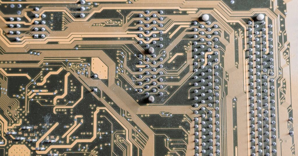
PCB design and layout encompasses the essential steps in creating printed circuit boards, which serve as the backbone of electronic devices. This process includes schematic capture, layout design, and design verification. Engineers focus on component placement, routing traces, and optimizing for performance and manufacturability.
Schematic capture involves translating circuit requirements into a visual representation. Designers create diagrams that represent electrical connections, ensuring that all components interact correctly. Accurate schematics prevent potential errors during manufacturing.
Layout design follows, where engineers arrange components on the PCB surface. Thoughtful placement reduces interference and improves signal integrity. Designers often use software tools to help visualize and simulate the layout, adjusting as necessary to meet design criteria.
Routing traces connects the components, forming electrical paths. Effective routing minimizes the length of connections while balancing layers and space constraints. Designers consider factors such as impedance, capacitance, and inductance during this phase, as these factors impact overall performance.
Design verification entails a thorough review of the design to catch any potential issues. Engineers utilize Automatic Design Rule Checking (DRC) tools to ensure compliance with industry standards. Testing the PCB design through simulations identifies faults before production.
Incorporating industry best practices during PCB design and layout results in reliable and efficient devices. By focusing on effective communication and collaboration among team members, designs can achieve the required functionality while conforming to timelines and budget constraints.
Importance of PCB Design and Layout
PCB design and layout are vital for electronic devices, directly impacting their reliability and efficiency. A robust design ensures devices function as intended while minimizing potential issues.
Functionality and Performance
Effective PCB design maximizes functionality and boosts performance. Strategic component placement enhances signal integrity, reducing interference and optimizing electrical pathways. When engineers utilize design software, they can simulate different layouts to investigate their impact on performance metrics like impedance. Thorough design verification processes help identify issues before production, enhancing end-user satisfaction with reliable operation. Well-executed designs facilitate smoother communication between components, leading to better overall performance in electronic applications.
Cost Efficiency
Cost efficiency plays a crucial role in PCB design. Thoughtful layouts reduce material waste by optimizing component placement and trace routing. Using efficient manufacturing processes can lower production costs significantly. Selecting cost-effective materials while ensuring quality also contributes to budget management. Implementing design best practices fosters a balance between high performance and low costs, making projects more financially viable. Thus, a focus on cost efficiency in PCB design ultimately leads to improved profit margins and competitive products in the market.
Key Components of PCB Design and Layout
Understanding key components is essential for effective PCB design and layout. These elements profoundly influence the completed board’s functionality and reliability.
Schematic Design
Schematic design represents the first step in PCB creation. Engineers translate electrical requirements into visual diagrams, establishing connections between components like resistors and capacitors. Clarity in this stage prevents future manufacturing issues. The process involves identifying each component’s role in the circuit, creating a comprehensive representation. Tools for schematic capture enhance accuracy and speed. A well-crafted schematic lays the foundation for successful layout design, ensuring that component interaction meets performance expectations.
Layout Design
Layout design focuses on positioning components on the PCB for optimum performance. Engineers strategically arrange elements while considering signal integrity and reducing interference. Each trace plays a critical role in guiding electrical signals efficiently. During this phase, software tools assist in visualizing space utilization and routing options. Minimizing trace lengths and optimizing pathways enhance overall electrical performance. Consideration of factors such as impedance and capacitance impacts the final design. The layout’s effectiveness directly influences a device’s reliability and functionality, ultimately affecting user satisfaction.
Best Practices for PCB Design and Layout
Implementing best practices in PCB design and layout enhances device functionality and reliability. Attention to detail during each design phase leads to significant improvements in performance.
Component Placement
Strategic component placement is vital for optimal PCB performance. Positioning components close to their connecting traces minimizes signal delays and reduces interference. Prioritizing critical components, such as power supplies and sensitive chips, helps to streamline signal flow. Properly organized components also facilitate easier routing and future troubleshooting. Engineers commonly utilize grid-based layouts to maintain alignment and standardize spacing while maximizing available board space.
Signal Integrity
Ensuring signal integrity directly impacts overall device performance. Keeping trace lengths consistent and avoiding sharp angles minimizes potential signal degradation. Engineers often implement differential pair routing for critical signals, which enhances noise immunity. Shielding sensitive signal traces with ground planes provides added protection against electromagnetic interference. Regular simulation and analysis throughout the design phase help identify and rectify potential signal integrity issues before production begins.
Thermal Management
Effective thermal management is crucial for maintaining device reliability. Proper thermal dissipation techniques prevent overheating and extend component lifespan. Components generating significant heat should be positioned away from heat-sensitive parts to mitigate thermal stress. Implementing adequate copper pour areas and thermal vias aids in dissipating heat effectively. Regular thermal simulations ensure that the layout supports proper heat management strategies throughout the operating range of the device.
Common Challenges in PCB Design and Layout
PCB design and layout present several challenges that can impact project outcomes. Understanding these obstacles is vital for effective design.
Design Complexity
Design complexity often arises due to the increasing functionality demands of modern devices. Engineers must contend with intricate circuitry that includes numerous components, leading to potential layout challenges. Managing signal integrity remains critical, especially as high-speed signals traverse compact PCBs. Component density also plays a significant role, necessitating precise placement to minimize interference. Complexity increases when integrating multiple layers, making it essential to ensure proper routing to avoid crosstalk. Complexity management tools offer assistance, but staying organized throughout the design process is key.
Manufacturing Constraints
Manufacturing constraints impose additional challenges during PCB design and layout. Fabrication technology often limits layer counts and trace widths. Engineers must align their designs with these constraints to ensure manufacturability without compromising performance. Costs can escalate if designs require specialized manufacturing processes. A careful selection of materials also impacts production efficiency and budget. Avoiding overly complex geometries helps facilitate easier assembly processes, thus enhancing the overall yield. A thorough understanding of manufacturing capabilities allows engineers to produce effective, reliable designs while adhering to industry standards.
Conclusion
Mastering PCB design and layout is vital for anyone looking to excel in the electronics field. A well-executed design not only enhances device reliability but also boosts performance and user satisfaction. By prioritizing best practices and leveraging advanced tools, engineers can navigate the complexities of modern circuitry while adhering to budget and timeline constraints.
Attention to detail in component placement and thermal management can significantly impact the overall efficiency of a product. As technology continues to evolve, staying informed about industry standards and manufacturing capabilities will be essential for creating innovative and effective PCB designs. Embracing these principles ensures that electronic devices meet the demands of today’s market while maintaining high-quality standards.